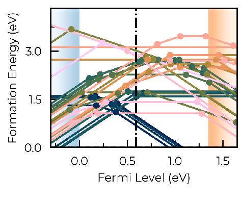
Hello, I would like to ask for help regarding an adjustment I’ve been trying to implement using doped. Having performed several defect calculations using the PBE functional, I would now like to adjust the band gap to match an HSE band structure calculation by shifting the VBM and CBM by -0.3 ev and 0.2 eV, respectively. Before my attempts to apply this asymmetric shift, the formation energy diagram for my system was this:
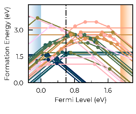
First, I tried redefining ‘vbm’ and ‘band_gap’ on DefectThermodynamics to match the desired values, but I only observe a shift in the CBM, while the VBM shows no significant change. Since the band extrema affect carrier concentration, I have also tried to apply this asymmetric shift to the DOS by creating a modified/asymmetric version of the ‘scissor_dos’ funcion or by manually changing the DOS values in the vasprun file, but I understand the problem with the VBM remains in the formation energy diagram, as it can be seen below. If we compare the positions of the charge transition levels near the VBM in both images, it seems like the VBM has shifted very little while the CBM has moved a lot more.
I would like to know if there is any other way these changes can be implemented consistently within doped so that I can obtain reliable results for the fermi level, carrier concentrations and the formation energy diagram. I greatly appreciate your help.
Hi Luis,
Nice formation energy diagram!
We generally advise against GGA-to-hybrid band shifting, if it can be avoided, given the range of issues it can bring ( Guidelines for robust and reproducible point defect simulations in crystals | Materials Chemistry | ChemRxiv | Cambridge Open Engage ).
As such, we do not natively support it with simple functions, but regardless it is possible to implement shifting in doped with whatever the chosen approach is – there are a number of methods as I guess you know.
For your approach of just modifying the vbm and band_gap, we have the bulk_band_gap_vr option in the DefectsParser methods for this. Why it’s only changing the gap and not the VBM in your case, I believe is because of this behaviour described in the docstrings:
vbm (float):
VBM eigenvalue to use as Fermi level reference point for
analysis. If ``None`` (default), will use ``“vbm”`` from the
``calculation_metadata`` dict attributes of the parsed
``DefectEntry`` objects, which by default is taken from the
bulk supercell VBM (unless ``bulk_band_gap_vr`` is set during
parsing). Note that ``vbm`` should only affect the reference
for the Fermi level values output by ``doped`` (as this VBM
eigenvalue is used as the zero reference), thus affecting the
position of the band edges in the defect formation energy plots
and doping window / dopability limit functions, and the
*reference of the reported Fermi levels.
*
So changing vbm after creating DefectThermodynamics doesn’t affect the defect entries that have already been parsed with the other vbm setting. If you confirm that this is the issue (by instead editing the calculation_metadata attributes or using bulk_band_gap_vr) I can add a catch for this in the code.
Hello, Seán.
Indeed, setting bulk_band_gap_vr during parsing was the way to effectively redefine the vbm. The CTLs now lie inside the band gap, as I had previously hoped. Of course, I assume the same shift has to be applied to the DOS, since it is used by doped to calculate carrier concentration and the fermi level. Thank you very much for your time and support.
1 Like