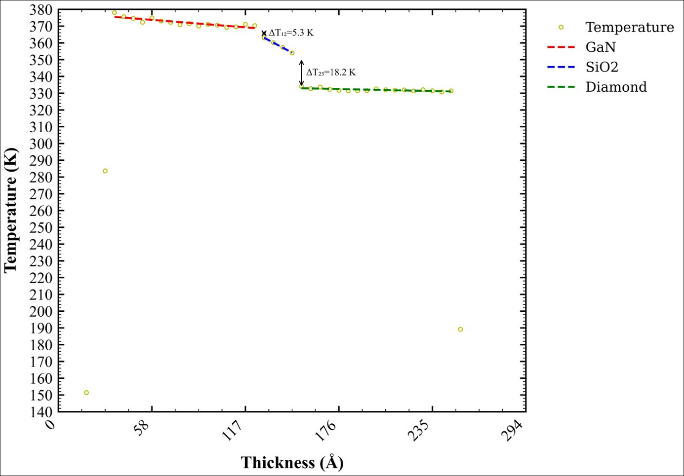
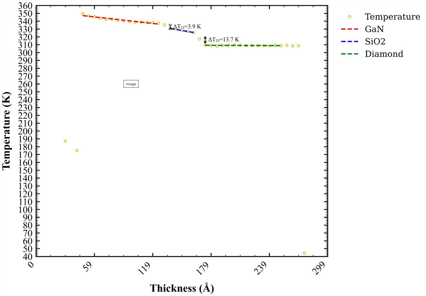
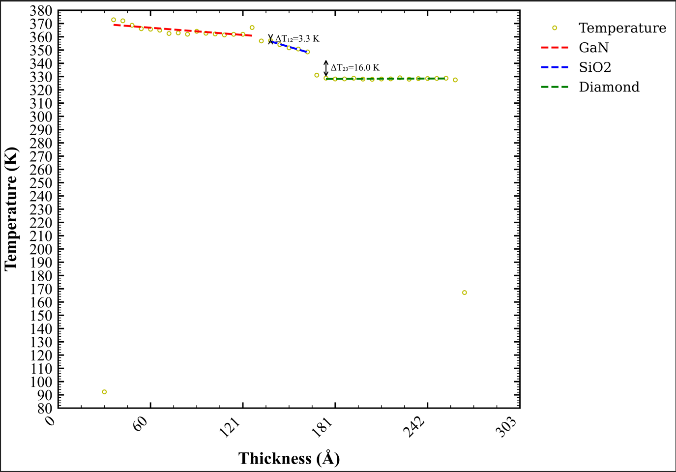
I am using LAMMPS to measure the interfacial thermal resistance of a GaN–SiO₂–Diamond heterostructure, in which the SiO₂ is purely crystalline rather than amorphous. I am investigating how varying the thickness of the interfacial layer affects the thermal resistance. My timestep is 1 fs, and I have prepared interfacial layers of 2.5, 3.0, 3.5, 4.0, and 4.5 nm. First, I performed relaxation of the model—constructed in Materials Studio—with 200 000 steps each of fix npt and fix nvt. I observed that the interface remained bonded and all thermodynamic parameters reached equilibrium. Next, I designated 10 Å–thick regions at the Diamond and GaN ends as adiabatic layers. After that, I ran 500 000 steps of fix nve together with fix ehex (using nevery = 1 and F=0.778 eV/ps) to establish a steady heat flux, and then collected 100 000 steps of averaged temperature data. I used ave/chunk and ave/time to plot the temperature gradient. However, I observed that as the interfacial layer thickness increased, the measured interfacial thermal resistance actually decreased. Moreover, the temperature difference across the interface was not pronounced—is this perhaps because the applied heat flux FFF is too small? Below are the temperature profiles for interfacial layer thicknesses of 2.5 nm, 3.0 nm, and 3.5 nm. Could someone help analyze the possible reasons? Is there an issue with my simulation procedure, or does this trend reflect a real physical effect?
We cannot answer your questions, but you likely can. When you want to know if something is a real effect, the answer is to be more rigorous with your measurement statistics. What is your uncertainty? How does that compare to the case of “no effect”?
More qualitatively, what trend do you expect from the literature on this topic? Are your results consistent with those expectations?
If you think something is off with your result, then you can also revisit your methods. You’ve defined a series of protocols to establish a steady-state thermal gradient. Have you confirmed that your protocol does this for all your cases? How do you know 100,000 timesteps is sufficient time.
Last, remember that by creating a small system in MD, you are making many approximations. In bulk crystals, both phonons and electrons contribute to thermal conductivity. Here you have only phonons. Also, your system geometry only permits short wavelength phonons. I’m not sure if that is expected to influence your measurement, but it’s good to keep in mind either way.