The definition of "doping" in Amset

Dear developer,
When I try to run the example, Si, in Amset, I found that setting the doping option to zero will fail the calculation.
I think a material which without doping should works.
I wonder how the “doping” works in Amset?
From the document, “Controls which doping levels (carrier concentrations) to calculate”.
Is this “doping” in Amset a real doping or carrier, such as electron or hole?
Does the mobility calculated from Amset from n- or p-type doping means the mobility of electron or hole?

Best,
John Chen
1 Like

Hi John,

The doping setting controls the concentration of charge carriers. A carrier concentration of zero implies that there are no carriers and therefore there can be no electronic transport. The sign of the doping indicates whether the carrier type is electrons or holes. Negative concentrations indicate electrons (n-type doping), positive concentrations indicate holes (p-type doping).

Best,
Alex

1 Like

Thank you, Alex.
It helps a lot.

Dear,
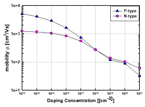
I tried the negative and positive doping settings, T=300, the results are plot here.
amset_si
I got very high hole mobility, I think it should be less than electron’s.

Is there any settings I lost?

Best,
John Chen

Could you please copy-paste your input file?

Dear,
This is input file:

scattering_type: [IMP, ADP]
doping: [-1E21,-1E20,-1E19,-1E18,-1E17,-1E16,-1E15,-1E14]
#doping: [1E21,1E20,1E19,1E18,1E17,1E16,1E15,1E14]
temperatures: [300]
bandgap: 1.14

interpolation_factor: 50

deformation_potential: deformation.h5
elastic_constant:
  - [144,  53,  53,  0,  0,  0]
  - [ 53, 144,  53,  0,  0,  0]
  - [ 53,  53, 144,  0,  0,  0]
  - [  0,   0,   0, 75,  0,  0]
  - [  0,   0,   0,  0, 75,  0]
  - [  0,   0,   0,  0,  0, 75]
static_dielectric:
  - [11.7, 0, 0]
  - [0, 11.7, 0]
  - [0, 0, 11.7]
high_frequency_dielectric:
  - [11.7, 0, 0]
  - [0, 11.7, 0]
  - [0, 0, 11.7]

write_mesh: true

I presume those results are for the Silicon example? To get good hole mobility values for Silicon, the calculations (deformation potential and band structure) must be computed with spin-orbit coupling included. Additionally, the dense mesh needs to be denser than that required for electrons.

If you do both of these things, then the hole mobilities will decrease significantly.

Dear Chen,

PRB 94, 085204 (2016) tells that it around thousands cm^2/Vs in mobility. I guess the calculation is not converged. Please try double the kmesh. For SOC effect suggested by Alex, I am not sure how large effect on there. Could you measure it?

Dear,
Thank you for response.
I will do more test about this.

One question I am still confused if you increase the kmesh to converge the results, the pymatgen Wavecar class will tell an error since it has a small limation of the size of the wavecar. To be frank, I think more mesh should be allowed to capture accurate results. How do you think?

Best wishes,
Zhibin

The size of the WAVECAR should not be too big in this case because silicon only has a few atoms and you can keep symmetry on. How large are the files that are being produced?

Also, please note that you can use the interpolation_factor setting to control the density of the interpolated mesh.

Lastly, the mesh used to generate the wavefunctions does not have to the same as the mesh used to generate the vasprun.xml used for Fourier interpolation of the bands. For example, you could generate the wave-function coefficients on an 10x10x10 mesh but use a 20x20x20 mesh to generate the dense electronic structure.

Best,
Alex

Dear Scientist Alex,

I seem to understand the meaning. I will try to use the interpolation-factor as you suggested.
Thank you very much!

Best,
Zhibin